From being a slogan, semiconductor self-reliance has graduated into a well-structured program under the India Semiconductor Mission. The Ministry of Electronics and Information Technology-launched ambitious initiative now looks to bring fabrication or advanced chip manufacturing to Indian soil for the very first time. Fiscal support by the government, up to 50 percent of the eligible project cost, ensures that large-scale semiconductor fabrication has been made possible without prohibitive risk by both domestic and foreign investors.
Unlike earlier, this is not a scattershot attempt. Every project under ISM undergoes multi-layered technical and financial scrutiny to ensure world-class competitiveness. The Union Cabinet, as of August 2025, approved ten projects cumulatively investing about ₹1.60 lakh crore, according to official statements from the Press Information Bureau and ISM. These range from wafer fabs and compound semiconductor units to testing and packaging facilities, making for a diversified base on which India can build its long-term semiconductor ecosystem.
From Intent to Infrastructure
Some of the first concrete steps include Tata Electronics’ semiconductor assembly and test facility in Jagiroad, Assam, which was announced in February 2024 with an investment of ₹27,000 crore. This marks India’s entry into the OSAT space. This project, supported by the Assam government and Tata’s technology partners, will be set up for assembling and testing chips meant for both domestic and export markets.
This is more than an investment in industry; it is a regional economic experiment. For Assam and the North-East, long excluded from high-technology manufacturing, the project signals a possible economic pivot. It aims at integrating a largely agrarian workforce into advanced assembly operations to create technical employment and a linked supply chain that can sustain long-term regional growth.
Equally significant is the HCL–Foxconn joint venture in Jewar, Uttar Pradesh, which was approved in mid-2025. The plant will have the capacity to handle approximately 20,000 wafers per month for display driver chips, used in mobile phones, cars, and smart home devices. This project is expected to be operational anytime between 2026 and 2028, based on public Cabinet records and company announcements. With Foxconn’s manufacturing pedigree and HCL’s engineering base, it represents a deliberate attempt to bridge India’s design and fabrication gap.
Building the Ecosystem
What differentiates the ISM from previous policy initiatives is the provision of a structured ecosystem beyond mere financial incentives. Support for display fabs, compound semiconductors, and advanced packaging is part of the mission’s architecture, with separate schemes and approval criteria in place. This is also similar to the approach taken by Taiwan’s Industrial Technology Research Institute, or ITRI, whereby state facilitation complements private enterprise.
Technology transfer and skilled manpower remain the hard parts of this transition. India has design talent, but fabrication requires a totally different operational discipline-cleanroom expertise, yield management, and precision logistics. ISM’s emphasis on capacity building through partnerships with global players is aimed at bridging this skill gap. These collaborations are critical because chip fabrication is as much about process knowledge as it is about investment.
At the same time, India’s semiconductor program is embedded in a geopolitical context. The global chain of chip supply has turned increasingly fragile after the disruptions of 2020-2021. A common factor underlying the U.S. CHIPS Act, the European Chips Act, and even Japan’s latest semiconductor incentives is diversification of production and reduction of over-reliance on East Asia. In that sense, India’s entry is not an isolated development; it forms part of a global rebalancing where resilience counts as much as efficiency does.
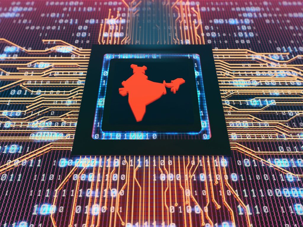
Image Source: Internet
Challenges of Scale and Credibility
Yet, challenges persist. Building and operating a semiconductor fab is capital-intensive and takes time. Even with generous fiscal support, projects take years to become operational. Energy stability, clean water access, and skilled technicians are all preconditions for sustained fabrication activity. Furthermore, semiconductor manufacturing is an ecosystem business and it cannot survive in isolation from suppliers of chemicals, gases, and precision machinery.
Another challenge will lie in keeping the transparency between policy ambition and actual implementation. India has already witnessed several semiconductor proposals come and go with much fanfare. The ISM must ensure every approved project keeps pace according to its schedule on land acquisition, environmental clearance, and supply chain integration. Only then will the narrative turn from policy to production.
The Road Ahead
Despite the hurdles, India’s semiconductor push marks an inflection point. The country is no longer content being a software and design powerhouse; it wants a share of the hardware manufacturing chain. If these current projects materialize on schedule, India will emerge, not as a competitor to Taiwan or South Korea, but as a credible supplementary hub.
This gradualist model-mixing fiscal prudence with institutional learning-could define India’s path ahead. Rather than race towards quick wins, ISM seems to be laying foundations that can sustain the sector through future technology cycles.
India’s semiconductor journey has barely begun, but the direction is unmistakable. It is this combination of state backing, corporate commitment, and global collaboration that lends credibility to the mission. The real test of India’s industrial maturity lies in the measured pace of this transition.
Sources:
1. India Semiconductor Mission (ISM) official scheme pages (ism.gov.in)
2. Press Information Bureau (PIB) releases, August 2025
3.Tata Electronics press release, 29 February 2024 (Jagiroad OSAT)
4. Reuters report on HCL–Foxconn semiconductor project approval, May 2025
Clear Cut Livelihood Desk
New Delhi, UPDATED: Nov 03, 2025 01:20 IST
Written By: Janmojaya Barik

Your article helped me a lot, is there any more related content? Thanks!
Sure. Kindly visit our digital platform (https://clearcutmedia.co.in/) to read more such stories.