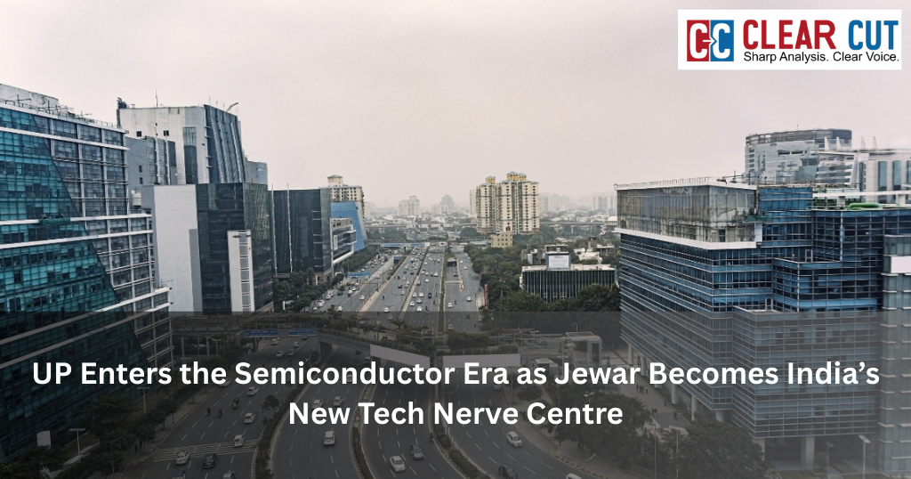
Uttar Pradesh has launched North India’s first semiconductor OSAT plant in Jewar with a ₹3,700 crore investment. The HCL–Foxconn India Chip project will produce 36 million display driver chips per month, strengthening India’s electronics supply chain.
Uttar Pradesh has taken a decisive step into India’s semiconductor journey. At Jewar in Greater Noida, Chief Minister Yogi Adityanath laid the foundation stone of North India’s first semiconductor project, India Chip. Backed by an investment of more than ₹3,700 crore, the project marks a turning point for the state’s industrial and technology landscape.
Addressing the gathering, the Chief Minister said the initiative reflects the long-term national vision of Prime Minister Narendra Modi. He stated that India is moving steadily towards becoming a global economic powerhouse, with advanced manufacturing and emerging technologies at its core. According to him, Uttar Pradesh has aligned itself with this vision by focusing on scale, speed, and policy-driven development.
What the Semiconductor Project Involves
The Jewar facility is a display driver semiconductor OSAT unit. OSAT refers to Outsourced Semiconductor Assembly and Test. This means the plant will not manufacture silicon wafers from scratch. Instead, it will assemble, package, and test display driver chips that are critical for smartphones, televisions, laptops, automotive displays, and industrial screens.
The project is being developed as a joint venture between HCL Technologies and Foxconn. Foxconn brings global expertise in electronics manufacturing and semiconductor packaging, while HCL anchors the venture through Indian operations and long-term localisation.
The unit is coming up in the Yamuna Expressway Industrial Development Authority area, close to the upcoming Noida International Airport. Officials said the location offers strong logistics connectivity, proximity to Delhi-NCR markets, and access to an existing electronics manufacturing ecosystem.

Why the Jewar Project Matters
Union Minister for Electronics and IT Ashwini Vaishnaw said the plant will have a production capacity of around 36 million chips per month once fully operational. He described the occasion as historic and said the facility would strengthen India’s electronics supply chain.
The chips produced at Jewar will primarily serve mass-market electronics. Officials said this will help reduce India’s dependence on imported display driver chips and support the country’s rapidly growing mobile phone and consumer electronics manufacturing base.
The project fits into India’s broader semiconductor strategy, which focuses on building assembly and testing capacity as a foundation before moving into full-scale fabrication. Policymakers see OSAT units as essential for developing skilled manpower, supplier ecosystems, and operational know-how.
From Disorder to Industrial Hub
Yogi Adityanath highlighted Jewar’s transformation over the past few years. He said that before 2017, the region was known for disorder and insecurity, with limited economic activity. Today, it is emerging as a major industrial node. He described Jewar as the new “Jewel of India,” driven by infrastructure projects, expressways, and investment-friendly governance.
The Chief Minister said Uttar Pradesh has introduced more than 34 sectoral policies since 2017. These include reforms aimed at easing compliance, improving transparency, and reducing legal friction for businesses. He added that under decriminalisation efforts, over 13 percent of criminal provisions across 99 state laws have been removed.
Leaders Back the Project
Prime Minister Narendra Modi, who joined the event virtually, recalled his remark from Semicon India that oil was once considered black gold, but chips are now digital diamonds. He said semiconductor capability will shape economic strength and technological sovereignty in the 21st century.
HCL Group Chairperson Roshni Nadar Malhotra said the project marks a new chapter in HCL’s growth journey. She expressed gratitude to both the central and state governments for their support and said the investment strengthens India’s technology and manufacturing ecosystem. She added that deepening HCL’s presence in Uttar Pradesh reflects confidence in the state’s governance and policy stability.
Foxconn Semiconductor Business Group President Bob Chen said the joint venture demonstrates how global manufacturing standards can be effectively localised in India. He said Foxconn’s build-operate-localise model focuses on skill development, local vendor integration, and community engagement.
Laying the Groundwork for Long-Term Growth
The Jewar semiconductor unit is expected to generate significant high-skill employment once operations begin. Officials associated with the project said the facility will create demand for electronics engineers, chip testing specialists, equipment operators, and quality control professionals, along with indirect jobs in logistics, precision tooling, packaging materials, and maintenance services. They added that OSAT facilities serve as critical entry points for building domestic semiconductor capability, as they help develop operational expertise, skilled manpower, and supplier ecosystems before countries move into advanced fabrication.
Foxconn Semiconductor Business Group President Bob Chen said the joint venture reflects a long-term commitment to localisation rather than short-term assembly. He said Foxconn’s build-operate-localise model focuses on training local talent, integrating Indian vendors into global supply chains, and embedding manufacturing capability within the region. HCL Group Chairperson Roshni Nadar Malhotra said the project marks a new phase in HCL’s growth journey and strengthens India’s technology and manufacturing ecosystem, adding that the company’s expanded presence in Uttar Pradesh reflects confidence in the state’s governance and policy stability.
Chief Minister Yogi Adityanath said the foundation stone laying is not merely the launch of an industrial unit but a symbol of technological self-reliance for a new India and a new Uttar Pradesh. Union Electronics and IT Minister Ashwini Vaishnaw said the project sends a strong signal to global investors and reinforces India’s push to reduce dependence on imported display driver chips. State officials said the facility firmly places Uttar Pradesh on the global semiconductor map and strengthens the electronics manufacturing corridor emerging across Jewar, Noida, and Greater Noida.
Clear Cut Startups Desk
New Delhi, UPDATED: Feb 22, 2026 02:30 IST
Written By: Ayushman Meena